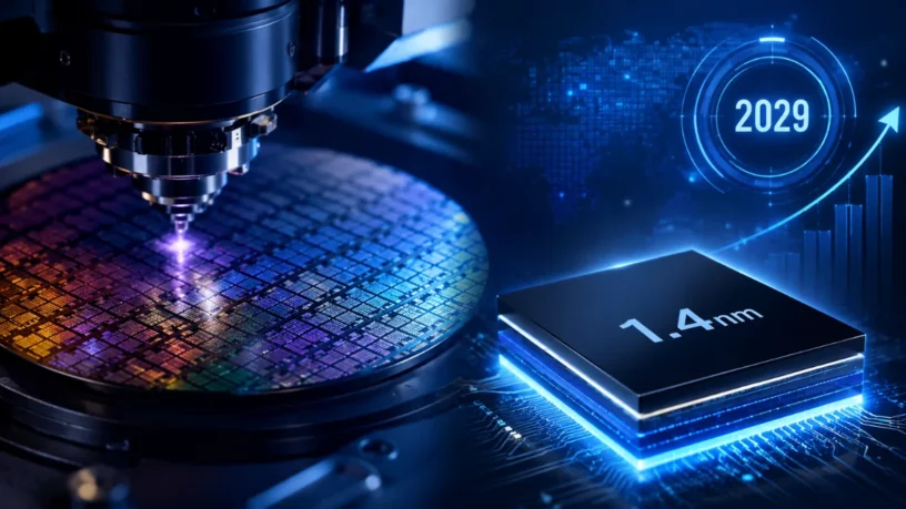
Samsung Electronics is moving ahead with the development of its next-generation 1.4nm foundry process after shifting its commercial production timeline to 2029, according to a report by South Korean financial publication The Bell. The company has reportedly begun sharing process plans with key semiconductor equipment suppliers as work on the advanced manufacturing node resumes.
The renewed effort follows Samsung’s decision to prioritize the maturity of its 2nm technology rather than pushing aggressively toward a smaller manufacturing node. That strategy appears to have given the company more room to stabilize yields before investing heavily in its next long-term process technology.
Equipment partners begin early development
According to The Bell, Samsung recently asked major semiconductor equipment makers, including Applied Materials and Lam Research, to begin early development of tools to support its 1.4nm manufacturing process. Those systems are expected to be installed at Samsung’s NRD-K research facility, the company’s advanced semiconductor R&D center in Giheung, South Korea.
Early collaboration between chipmakers and equipment suppliers is standard practice for leading-edge semiconductor manufacturing. Process requirements are typically defined years before mass production, allowing equipment vendors to tailor deposition, etching, and inspection tools to the technical demands of each new node.
The report also states that Samsung has already brought ASML’s High-NA EUV lithography system into the NRD-K facility. High numerical aperture EUV is widely expected to play a role in manufacturing beyond today’s most advanced nodes by improving patterning precision for extremely small transistor features.
Focus first shifted to 2nm
Samsung originally planned to commercialize its 1.4nm process much earlier, but later delayed mass production to 2029. The company instead focused on improving its 2nm SF2 platform and derivative processes, aiming to strengthen manufacturing yields and attract major foundry customers.
That decision may already be paying off. Samsung has recently secured high-profile AI chip manufacturing business while continuing to improve the competitiveness of its advanced foundry offerings, giving the company a stronger foundation before moving to an even more challenging technology generation.
The delay also reflects the growing complexity of semiconductor manufacturing. Every new node requires tighter process control, new materials, and increasingly sophisticated lithography equipment, resulting in longer, more expensive development cycles than in previous generations.
Competition remains intense
Samsung’s renewed push comes as the semiconductor industry races toward sub-2nm manufacturing. TSMC is targeting commercial 1.4nm-class production around 2028, while Intel is also pursuing its own advanced process roadmap.
Beyond logic chips, The Bell reports that Samsung has also begun requesting equipment for development of its next-generation V12 NAND flash memory, which is expected to enter mass production around 2030. Future memory technology is expected to use more advanced wafer-stacking techniques to increase storage density and improve performance.
Whether Samsung can narrow the technology gap with TSMC will depend on more than reaching the 1.4nm milestone. Manufacturing yields, production costs, customer adoption, and the successful deployment of High-NA EUV equipment will likely determine how competitive the company’s next generation of foundry technology becomes when it reaches commercial production.